6502 Hack Day Build

Details

I always wanted to build a 6502 based computer.

The 6502 is the chip used in all sorts of computers throughout history, ranging from the Apple II, the NES, and the Commodore 64… all of the way through to the Terminator and Bender.

I’ve drawn a bunch of attempted schematics, never really bothered to build any of them.

I’ve had the requisite chips sitting around since 2008 or so.

Eventually, early in 2019, there was a hack day and, since my past experiences with hack days have frequently left a bad taste in my mouth, I decided that I’d support the idea of doing a hack day by doing something completely useless… A 6502 breadboard computer.

I was mostly inspired by Dirk Grappendorf’s really quite nice 6502 build, especially how he provided a nice suite of test firmware, so a lot of my design is inspired by that build or Daryl’s SBC2.

I ran into some problems, learned some hard lessons about breadboarding, and kept going after the hack day.

GitHub repo
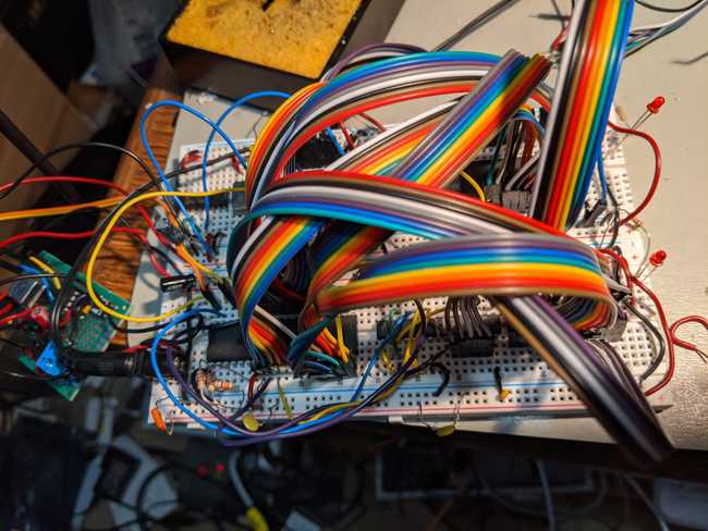
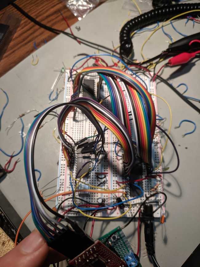
Build Log

Step 6: Where I reach the limits of the breadboard

Goal: Make sure the board won’t asplode when I plug it in.

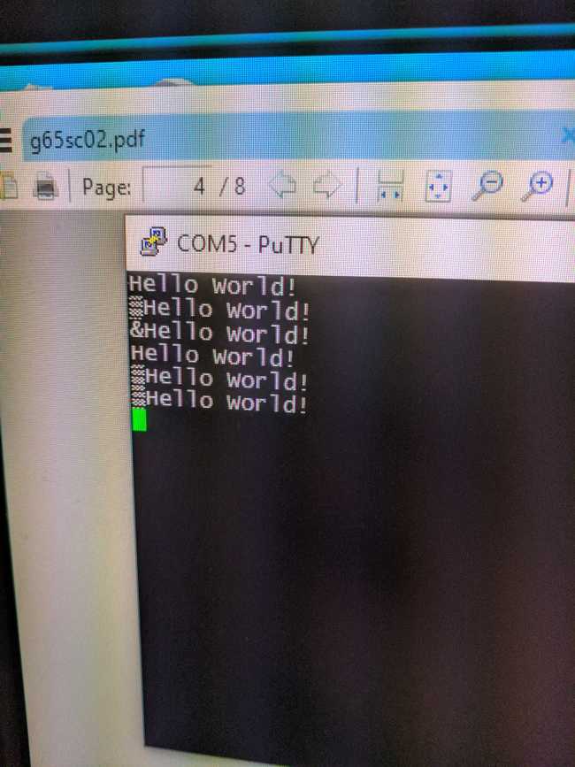
I managed to not break the board after not working with it since last August. I did a careful check, made sure the wires weren’t plugged wrong, etc. After doing a bunch of checks, I plug it in, connect to the serial port, and it says ”▒▒▒▒▒ ▒▒▒▒▒!” instead of “Hello World!”

It turns out that one of the wires between the 6551 serial controller and the 6502 had come loose. But, because it was so close to working, even though the firmware was setting that bit of a register, it was almost working.

Goal: Get RAM hooked up and IO decoded

The 6502 is really nearly useless without some RAM, maybe about 256 bytes for the zero page and 256 bytes for the stack page. Otherwise, all you’ve got is three registers to work with.

Most of the modern designs tend towards a relatively friendly and easy memory mapper circuit. We started out just using an inverter on A15 to select between the ACIA and the RAM, but now we’ve got two devices and they are very different sizes, so the usual approach is to put an 8-input NAND gate on A14 down to A8 to get a control line for the IO.

I was kinda following Dirk Grappendorf’s tutorial but I got myself slightly confused at the RAM part of things.

What it turns out worked better for me was to just wire up the complete set of IO decoders right away to mimic the SBC-2 design as well as a later section of Dirk Grappendorf’s tutorial before trying to hook up the RAM, because the 3-to-8 decoder is adding an invert step.

The memory map here is pretty much:

  • 0x0000-0x7EFF - The RAM
    • 0x0000-0x00FF - Zero Page
    • 0x0100-0x01FF - Stack page
    • 0x0200-0x7EFF - Available memory
  • 0x7F00-0x7FFF - IO, where the first few bytes are the ACIA
  • 0x8000-0xFFFF - The first 32k of the flash ROM

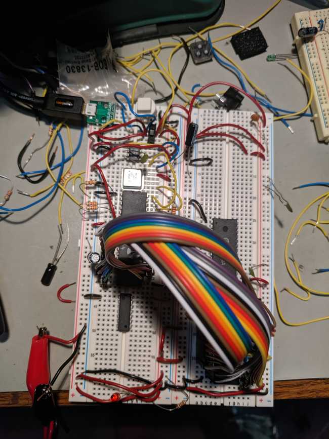
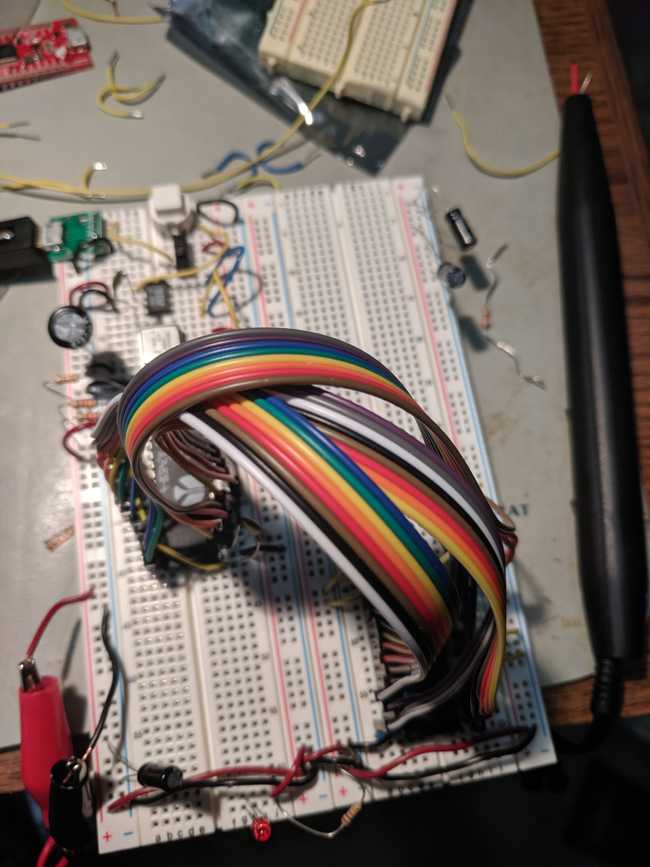
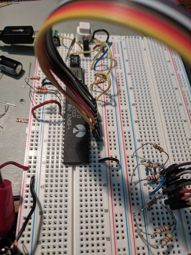
The whole works is getting way too unreliable at this point. Every time I add wires, I have to figure out what came loose.

Image

I think the next step is to design a PCB because then I don’t need to solder a bunch of 8-bit buses across a perfboard.

Step 5.3: A giant step back where things start to work

Image

I ended up getting a few things.

First, I got a cheap $10 logic analyzer that was supported by Sigrok. Second, I got a fresh set of chips from a different manufacturer, plus more ribbon cable so that it wouldn’t risk devolving too far into a rat’s nest.

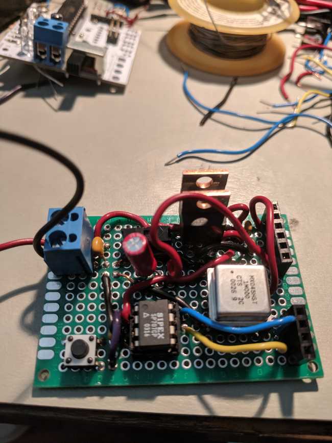
Third, I decided that I’d solder up a tiny little board with the power circuit, the switch, the reset button, and the CPU clock.

I did a quick test and it looked like for a bit that the single-step clock might be a problem because it was looking a lot more like it was properly looping when I hooked up the logic analyzer.

I ended up stripping the board of most of the wiring and starting over with a fresh set of parts, starting off from having just a CPU and a NOP-generator, through the part where it runs a loop in Flash RAM. I was able to use Sigrok to decode the values on the data bus and validate that it was doing the exact right thing.

Then I spent some time mucking around with serial lines, trying to make sure I had the right connections, and from there, I was finally able to get the serial port up.

Then I was able to go back and replace parts and determine that the 65c02 I had was somehow faulty. Not sure if it was always bad and somehow a defective part made it into the supply chain or if I’d zapped it at some point in the past.

Image

Image

Step 5.2: Single-step

Image

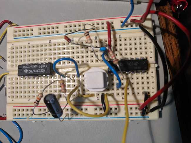
I wired up a single-step clock by the end of the hack-day weekend. This means that, instead of going at 1 MHz, I can clock one bit at a time.

Running the whole CPU + Flash RAM + ACIA stack: Inconclusive.

Running the whole CPU + Flash RAM + ACIA stack with the Flash in a tight loop: Why is the address line going in a weird direction? Also, why are some of the lines silent with my logic probe?

I check and the silent line is within the spec for that particular part against the Rockwell datasheet. Switch the logic probe to TTL mode and it starts to behave. But it’s going into places that it’s not supposed to be going!

Switching back to the configuration from Step 3, but single-stepping: Discover that the processor is very much not single-stepping properly anymore. Seems like somewhere along the way I managed to zap it!

It also turns out that I only picked up one 65c02, which is a really poor life choice.

Second break: Waiting for a 65c02 to appear in the mail!

Step 5.1: Voltage sag fix

Image

I tried a few things. It seemed to get a little bit better once I added duplicate power lines, but it was still floating around 4v - 4.2v. I checked and I’m “only” using 80 mA of power.

I tried every USB adapter I had around to see if it was a crappy adaptor.

I’m not sure if it’s a crappy breadboard or just all breadboards are like that.

I could have probably soldered up a point-to-point board, except I didn’t have the sockets for all of the part sizes, nor did I have a sufficently large board… and that whole process is annoying.

So, this is where the hack-day ended. But Hack Day is there till the end of the weekend, really.

Eventually, I asked on the adafruit discord and madbodger suggested and it was suggested to go to board-level regulation. So I wired up a 12v power supply, so the power switch switches 12 volts, and then put a pair of 7805 regulators, one for each board. And that got me to the point where I had happy 5v rails.

Step 5: Attempt to connect CPU + Flash RAM + ACIA + Simple address decoder and experience voltage sag

Goal: Get to the point where my desktop computer will talk to the 6502

In the days of yore, you’d wire up an RS232 port to your computer. This meant that you needed an extra chip to do the voltage conversion, generally a MAX232. These days, pretty much everyone standardized on the FTDI connector, which is 2 signal lines, the RX and TX lines, and power and ground, in a 6 pin header that all of the popular USB serial port breakout boards connect to.

So I get my USB serial breakout adaptor connected, the Flash RAM and the ACIA.

The memory map here is pretty much:

  • 0x0000-0x7FFF - The ACIA, repeated every 4 bytes
  • 0x8000-0xFFFF - The first 32k of the flash ROM

It didn’t work.

I had a few wires not correctly inserted into the right places, so I fixed that.

But the clock wasn’t getting output from the Phi-1 and Phi-2 pins, and everything was stopped.

It took me a while. I kept suspecting that the RESET line was the wrong one because it didn’t seem to be triggering. I figured out after a while that the power LED I’d helpfully added on the board felt dim, so I pulled the voltmeter out and realized that the voltage was around 3v, and the MAX707 triggers at 4.65V.

Step 4: CPU + Flash RAM

Image

Goal: Attach a device to the databus.

Okay, a few steps at once.

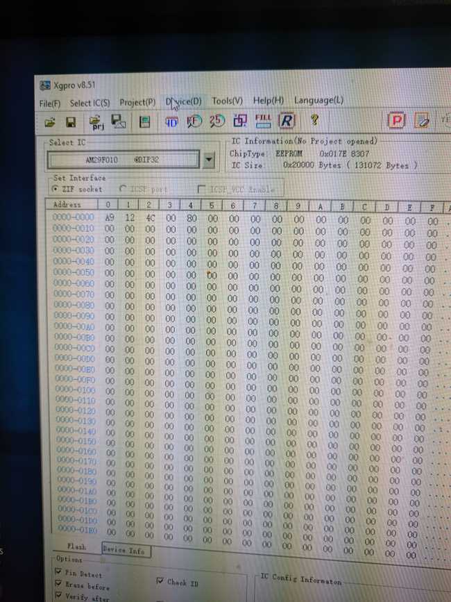
The goal is to have a relatively friendly modern build environment going. I found one project that was actually showing how to use cc65 and makefiles as your build environment. So that got me started on having a generated HEX file that I could burn to the ROM.

The Flash ROM has a slightly longer loop going.

The memory map here is pretty much:

  • 0x0000-0x7FFF - The first 32k of the flash ROM
  • 0x8000-0xFFFF - The first 32k of the flash ROM, mirrored

Image

Step 3: CPU going straight into a NOP generator

Image

Goal: Get the CPU free-running on a NOP instruction

There’s two ways to do this. One way is really simple but ever-so-slightly unsafe, the other way is much safer. You can either directly wire the binary pattern for a NOP instruction using wires to +5V and GND. Or you can put resistors there, so that it won’t fry if you get the bit pattern wrong and the CPU tries to write to the data bus.

I picked the second route, which means that D1, D3, D5, D6, and D7 all have a 4.7k ohm resistor to the +5V line and the three other lines (D0, D2, D4) are all tied to 47 ohm resistor on the GND line.

http://www.6502.org/mini-projects/nop-gen/nop-gen.htm

On Amazon, I got some ribbon cable that was already crimped to cute little one-pin housings. I’ve divided these into little 8 bit bus lines and I’m routing them to where the Flash RAM is eventually going to live.

Step 2: Clock

Goal: There must be a 1 MHz clock.

I’ve got a half-can TTL oscillator. Normally I manage to install them improperly because the dots are weird, so I had to look for the edge that’s not rounded off and use that as a reference.

A lot of people start off with a crystal oscillator. The problem with that is that you then wonder “Hey, did I do the oscillator right?” and goink with a capacitor somewhere in the 20 pF range and it sucks. I went for a oscillator because those are dead-simple by comparison.

Step 1: Reset Circuit

Start of hack day project

Goal: There must be a circuit that will reset the CPU when the power comes up and de-bounce the reset button.

For whatever reason when I picked up the bits, MAX707’s was a cheap microprocessor supervisor device that was available. It’ll send a reset pulse, it’s got an input for a button that it’ll debounce, it can send a brownout warning if you configure it right, and it’s got both inverted and regular RESET rails.

I used a USB breakout adapter to drive the 5v rails.

Step 0: Acquire parts

Image

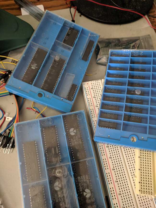
I’d purchased from Jameco a pair of 65C02’s, a pair of 65C22’s, a 6551, a MAX707 equivalent, plus some Am29F010 Flash RAM and some SRAM like ten years ago and it spent the years haunting me.

I’d intended to make my own Flash RAM burner but decided that was it’s own project, so I decided to borrow the design for an EEPROM burner and decided that I might as well just get one of those reasonably cheap device burners off of Amazon instead.

I also picked up some fresh breadboards because I didn’t want to evict my past project from it’s board just yet.

Posted:

Updated: